GrabCAD
Solar Charger PCB
by GrabCAD
Last crawled date: 1 year, 11 months ago
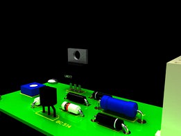
Solar Charger PCB with adjustable output and battery protection
Charging current passes through D1 to the voltage regulator LM 317. By adjusting its adjust pin, output voltage and current can be regulated.
A variable resistor (VR) is placed between the adjust pin and ground to provide an output voltage conducive with your battery voltageThe resistor R3 restricts the charging current and diode D2 prevents discharge of current from the battery. Transistor T1 and the Zener diode ZD act as a cut off switch when the battery is full.
When the terminal voltage of the battery rises above 6.8 volts, Zener conducts and provides base current to the transistor. It then turns on grounding to the output of LM 317 to stop charging.
Source : http://www.circuitdiagram.org/led_light_circuits_2.html
Similar models
grabcad
free

Voltage Regulator 7805 and Adjustable Voltage Regulator LM317
...17, are use to stabilize the voltage, 7805 for 5v and lm317 can be adjusted with resistors to output current from 1.25 v to 37 v.
grabcad
free

Linear Voltage Regulators 78XX
...e adjusted with resistors to output current from 1.25 v to 37 v.
https://www.instructables.com/member/robottronic/instructables/
grabcad
free

MPPT 5A Solar Controller DC-DC Step Down Buck Module, Const. Voltage & Current Converter
...nce the charging current to double. with a constant current and prevents battery overcharge, effective protection of the battery.
3dwarehouse
free

Variable impedance circuit
... of the transistor is varied with excellent linearity in accordance with the value of the voltage of the variable voltage source.
grabcad
free

Enclosure for Digital electronic part tester PCB
...tester pcb
grabcad
the casing or box for digital transistor, diode, resistor, capacitor meter. the battery is placed out of box.
3dwarehouse
free

LT3750
...ide sense—no output voltage divider necessary wide input range: 3v to 24v drives gate to vcc – 2v available in 10-lead ms package
thingiverse
free

Solar Panel Charge Circuit DC-DC Voltage Regulator
...solar panel charge circuit dc-dc voltage regulator
thingiverse
solar panel charge circuit dc-dc voltage regulator
grabcad
free

03962A (HW107) Lithium Battery Charging Module
...m damage or degrading life due to over-charge, over-discharge, over-current.
the mosfet smc8205 is a power management transistor
3dwarehouse
free

Solar battery charger
...rd or pcb soldering accessories further reading: how to make a (really) simple diy solar usb charger for your phone or mp3 player
thingiverse
free

USB Portable Battery Charger Box
...sb ports when completed. 5mm m2 screws hold the boards in place and the cover can be secured in any way you find works for you.
Pcb
turbosquid
$19

PCB assembly line.
...mbly line. for download as 3ds, max, ige, obj, stl, and sldas on turbosquid: 3d models for games, architecture, videos. (1330649)
3ddd
$1

GRAMERCY HOME - CARMELA ARMCHAIR 602.023-PCB
...gramercy home - carmela armchair 602.023-pcb
3ddd
gramercy home
gramercy home
carmela armchair
602.023-pcb
www.gramercy-home.ru
3d_export
$150

auto pcb board loder inspection machine
...auto pcb board loder inspection machine
3dexport
auto pcb board loder & inspection machine --> only step file
3d_export
$7

turning mechanism drawing pcb board turnover machine
...turning mechanism drawing pcb board turnover machine
3dexport
turning mechanism drawing pcb board turnover machine
turbosquid
$9

Stereo Jack 3.5mm for soldering to a PCB
... available on turbo squid, the world's leading provider of digital 3d models for visualization, films, television, and games.
3d_export
$5
LED Right Angled PCB Mounting
...m led. step and igus files. multiple led colors: blue, purple, red, green, and yellow. dimensions case w 4,5mm , h 7,3mm l 6,4mm.
3d_export
$20

automatic pcb loading and unloading dispensing test automatic line
...ment structure is very complex. it is a very practical equipment for smt industry. the equipment is mature application equipment.
3d_export
$18

an automatic line for fct function test of pcb
... drawings are downloaded, you can directly watch and edit the contents. welcome to download and learn from your favorite friends.
3d_export
$5

USB Micro B connector
...step and igus for 3d import into ecad tools, pcb footprints. added also a altium designer pcb component library...
3d_export
$15

plastic housing with dewalt battery holder
...case measures 155x106x60. inside the case there are two pcb of 130x98 and 98x42...
Charger
3d_export
$5
charger
...ers in battle. this is the 18th century meaning of charger, and it’s based on the verb charge and its meaning “rush into battle.”
3d_export
free
Charger
...charger
3dexport
turbosquid
$15

Charger
... available on turbo squid, the world's leading provider of digital 3d models for visualization, films, television, and games.
turbosquid
$3

Charger
...d model charger for download as skp, max, blend, stl, and obj on turbosquid: 3d models for games, architecture, videos. (1654816)
turbosquid
$1
charger
... available on turbo squid, the world's leading provider of digital 3d models for visualization, films, television, and games.
3d_export
$20

dodge charger 1972
...dodge charger 1972
3dexport
dodge charger 1972
3d_export
$20
dodge charger 1969
...dodge charger 1969
3dexport
dodge charger 1969
3d_export
free

dodge charger 1969
...dodge charger 1969
3dexport
dodge charger 1969
3d_export
$18

dodge charger
...dodge charger
3dexport
3d_export
$89
Charger 3D Model
...charger 3d model
3dexport
charger sea transopt industry 3d models
charger 3d model vitaly amurskiy 2286 3dexport
Solar
3d_ocean
$4

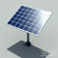
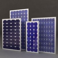
Solar Panel
...solar panel
3docean
cell panel solar
fully textured solar panel with scaleable solar cells.
3ddd
$1
solar cell
...solar cell
3ddd
солнечная батарея
solar cell
3d_export
$7

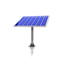
Solar Panel
...solar panel
3dexport
perfect solar panel for roof, modular, extensible.
3d_export
$5

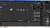
solar system
...solar system
3dexport
solar system in c4d, with 8k nasa textures
3d_export
$15
solar system
...nd the other the sun, the earth and the moon, the latter has an animation with camera movement included, the files are in spanish
3ddd
$1
Zumtobel Solar II
...obel solar ii
3ddd
zumtobel , solar
модель направленного светильника solar 2 от zumtobel
3d_ocean
$14
Solar Panels
... materials, hdri map, vray gi setup. four solar panels: type1: 1849 – poly, 2035 – vert. type2: 954 – poly, 1051 – vert. type3...
turbosquid
$29

Solar System
...squid
royalty free 3d model solar system for download as fbx on turbosquid: 3d models for games, architecture, videos. (1236050)
turbosquid
$25
Solar Panel
...osquid
royalty free 3d model solar panel for download as max on turbosquid: 3d models for games, architecture, videos. (1516562)
turbosquid
$25
Solar System
...uid
royalty free 3d model solar system for download as blend on turbosquid: 3d models for games, architecture, videos. (1314058)