Thingiverse
Printed Circuit Board (PCB) Vise by whitejd86
by Thingiverse
Last crawled date: 3 years, 1 month ago
My design goal was to produce a simple and useful concept.
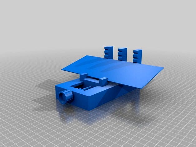
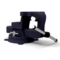
Vise developed for secure placement of a printed circuit board (PCB) while performing multiple operations (inspection, component installations, modifications, repair, etc.)
Overall dimensions: L = 182 mm / W = 86 mm / H = 80 mm
Flat placement and multiple tilt orientations permissible via numerous retention features.
Maximum grab width is 116 mm (at max tilt angle). Easy adjustment of securing load via knob-driven pusher.
Additional hardware (bolt, jam nuts, and washers) identified in graphics - exploded view.
Print Settings:
(1) Knob printed with 100% fill, and 30% fill used for Main Body and Pusher.
(2) Main Body printed with 0.15 mm layer height, 0.1mm layer height for Pusher & Knob.
(3) Additional settings shown in provided graphics (per Cura slicer screenshots).
Similar models
thingiverse
free

Very simple PCB vise by ByTechLab
...e: 0.4 mm
description of this project on my web page:https://bytechlab.com/2018/02/very-simple-pcb-vise/
some images and renders:
thingiverse
free

PCB Vise by ModelStation
... so that it will print on a tom and will hold circuit boards in such a way that you have better access to the edges of the board.
grabcad
free

IC for PCB
...ic for pcb
grabcad
this ic used in pcb (printed circuit board)
grabcad
free

test points printed circuit board
...ints printed circuit board
grabcad
through-hole test points for printed circuit boards. diameter solderhole pcb 1mm, height 5mm.
thingiverse
free

Ultimate PCB and IC Vise – Version 4 - Printable Vise for Small Electronics by GeoffreyG
...them. also, there are some important items to consider when building this vise, so be sure to see the notes i’ve provided below.
grabcad
free

PCB
...ok as aesthetic as possible. a printed circuit board (pcb) is a laminated sandwich structure of conductive and insulating layers.
grabcad
free

Logitech c920 PCB
... printed circuit board with accurate mounting holes and speaker placement. includes a (not very good) decal overlay of circuitry.
grabcad
free

Medical sensor. Case and 3D layout of the printed circuit board
...or. case and 3d layout of the printed circuit board
grabcad
the concept and design of the pcb and the body of the medical sensor
3dwarehouse
free

PCB
...pcb
3dwarehouse
printed circuit board
thingiverse
free

Panavise PCB Holder by mkellner
...a full set of parts. the pcb guide slots were squared off and an angle was applied to the base to give the arms a slight tilt in.

Vise
3d_export
$6

Machine vise
...machine vise
3dexport
machine vise
3d_export
$5
Machine vise
...machine vise
3dexport
machine vise
turbosquid
$2
Vise
...uid
royalty free 3d model vise for download as obj and blend on turbosquid: 3d models for games, architecture, videos. (1445802)
turbosquid
$10
Vise
...
royalty free 3d model vise for download as max, obj, and fbx on turbosquid: 3d models for games, architecture, videos. (1170628)
turbosquid
$40

Vise
... available on turbo squid, the world's leading provider of digital 3d models for visualization, films, television, and games.
turbosquid
$25

Vise
... available on turbo squid, the world's leading provider of digital 3d models for visualization, films, television, and games.
turbosquid
$19

Vise
... available on turbo squid, the world's leading provider of digital 3d models for visualization, films, television, and games.
turbosquid
$16
Vise
... available on turbo squid, the world's leading provider of digital 3d models for visualization, films, television, and games.
turbosquid
$15

Vise
... available on turbo squid, the world's leading provider of digital 3d models for visualization, films, television, and games.
turbosquid
$10
vise
... available on turbo squid, the world's leading provider of digital 3d models for visualization, films, television, and games.
Circuit
turbosquid
free

Circuit Board
...turbosquid
free 3d model circuit board for download as blend on turbosquid: 3d models for games, architecture, videos. (1279126)
turbosquid
$20

CIRCUIT BREAKER
... available on turbo squid, the world's leading provider of digital 3d models for visualization, films, television, and games.
turbosquid
$19
Circuit Breaker
... available on turbo squid, the world's leading provider of digital 3d models for visualization, films, television, and games.
turbosquid
$19
Circuit Breaker
... available on turbo squid, the world's leading provider of digital 3d models for visualization, films, television, and games.
turbosquid
$19

Circuit Breakers
... available on turbo squid, the world's leading provider of digital 3d models for visualization, films, television, and games.
turbosquid
free

Circuit Breaker
... available on turbo squid, the world's leading provider of digital 3d models for visualization, films, television, and games.
3d_export
$65

circuit board
...circuit board
3dexport
simple rendering of the scene file
archive3d
free

Circuit breaker 3D Model
...rcuit breaker schneider electric n240211 - 3d model (*.gsm+*.3ds) for interior 3d visualization.
turbosquid
$35

Short circuit key
...
royalty free 3d model short circuit key for download as 3ds on turbosquid: 3d models for games, architecture, videos. (1187722)
design_connected
free

Circuit 1 Sconce Lamp
...circuit 1 sconce lamp
designconnected
free 3d model of circuit 1 sconce lamp by apparatus
Pcb
turbosquid
$19

PCB assembly line.
...mbly line. for download as 3ds, max, ige, obj, stl, and sldas on turbosquid: 3d models for games, architecture, videos. (1330649)
3ddd
$1

GRAMERCY HOME - CARMELA ARMCHAIR 602.023-PCB
...gramercy home - carmela armchair 602.023-pcb
3ddd
gramercy home
gramercy home
carmela armchair
602.023-pcb
www.gramercy-home.ru
3d_export
$150

auto pcb board loder inspection machine
...auto pcb board loder inspection machine
3dexport
auto pcb board loder & inspection machine --> only step file
3d_export
$7

turning mechanism drawing pcb board turnover machine
...turning mechanism drawing pcb board turnover machine
3dexport
turning mechanism drawing pcb board turnover machine
turbosquid
$9

Stereo Jack 3.5mm for soldering to a PCB
... available on turbo squid, the world's leading provider of digital 3d models for visualization, films, television, and games.
3d_export
$5
LED Right Angled PCB Mounting
...m led. step and igus files. multiple led colors: blue, purple, red, green, and yellow. dimensions case w 4,5mm , h 7,3mm l 6,4mm.
3d_export
$20

automatic pcb loading and unloading dispensing test automatic line
...ment structure is very complex. it is a very practical equipment for smt industry. the equipment is mature application equipment.
3d_export
$18

an automatic line for fct function test of pcb
... drawings are downloaded, you can directly watch and edit the contents. welcome to download and learn from your favorite friends.
3d_export
$5

USB Micro B connector
...step and igus for 3d import into ecad tools, pcb footprints. added also a altium designer pcb component library...
3d_export
$15

plastic housing with dewalt battery holder
...case measures 155x106x60. inside the case there are two pcb of 130x98 and 98x42...
Board
archibase_planet
free
Board
...e planet
board information board bulletin board
board information n310813 - 3d model (*.gsm+*.3ds) for interior 3d visualization.
archibase_planet
free
Board
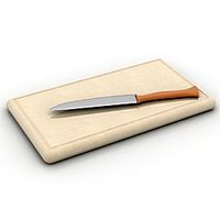
...board
archibase planet
board cutting board kitchen ware
board n051011 - 3d model (*.gsm+*.3ds) for interior 3d visualization.
archibase_planet
free

Board
...board
archibase planet
board blackboard school board
board school n290114 - 3d model (*.gsm+*.3ds) for interior 3d visualization.
archibase_planet
free
Board
...board
archibase planet
slate board
board - 3d model (*.gsm+*.3ds) for interior 3d visualization.
archibase_planet
free
Board
...board
archibase planet
blackboard board school furniture
board - 3d model for interior 3d visualization.
archibase_planet
free
Board
...board
archibase planet
board shelf stand
board - 3d model (*.gsm+*.3ds) for interior 3d visualization.
archibase_planet
free
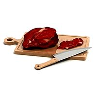
Board
...board
archibase planet
kitchen ware board
board - 3d model (*.gsm+*.3ds) for interior 3d visualization.
archibase_planet
free
Board
...board
archibase planet
kitchen ware board
board n150410 - 3d model (*.gsm+*.3ds) for interior 3d visualization.
archibase_planet
free

Board
...board
archibase planet
board office supplies stationery
board - 3d model (*.gsm+*.3ds) for interior 3d visualization.
archibase_planet
free

Board
...board
archibase planet
board gym
board evminov n240613 - 3d model (*.gsm+*.3ds) for interior 3d visualization.
Printed
design_connected
$27
...print
designconnected
moroso print computer generated 3d model. designed by wanders, marcel.
3ddd
free

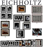
Eichholtz Prints
...- eichholtz print central station i
13 - eichholtz print central station ii
14 - eichholtz print marisa
15 - eichholtz print tish
3ddd
$1

Eichholtz Prints
...print abstract - set of 2
10 - eichholtz print orange abstract
11 - eichholtz print buddha right
12 - eichholtz print buddha left
turbosquid
$1

... available on turbo squid, the world's leading provider of digital 3d models for visualization, films, television, and games.
3ddd
free
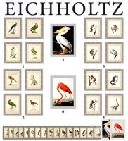
Eichholtz Prints
...of 4
2 - print dunbar 2 set of 4
3 - print guadeloupe 1 set of 4
4 - print guadeloupe 2 set of 4
5 - print giles
6 - print trett
3ddd
$1

Eichholtz Prints
...nt tutti frutti
3 - eichholtz prints watson - set of 2
4 - eichholtz prints antique nautilus - set of 2
5 - eichholtz print tiara
3d_export
$5
Monster for printing
...monster for printing
3dexport
monster 3d model printing
3ddd
free
printed rug
...printed rug
3ddd
ковер
very creative printed rug
3ddd
free
Eichholtz Prints
...иал: бумага
габариты (вхш): 72 x 62 см
описание: print sweetmeat - постер в деревянной раме.
3 - prints varsity set of 2
арти
3ddd
free
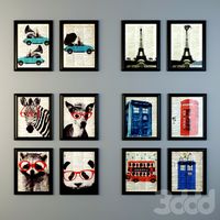
Art Print Posters
...art print posters
3ddd
прованс
art print posters by patrician prints